Explore lithography tools for nanoscale and microscale fabrication at the Materials for Opto/Electronics Research and Education (MORE) Center at Case Western Reserve University.
Electron Beam Lithography
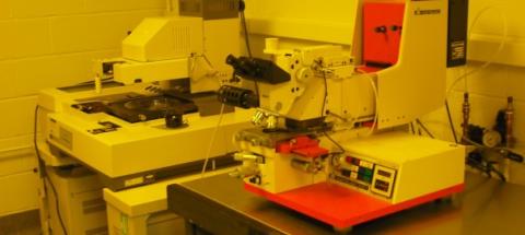
Tescan Vega-3 SBH
Electron beam (e-beam) lithography on our Tescan VEGA-3 uses a tightly focused, high-energy electron beam in a scanning electron microscope (SEM) to directly write patterns into an electron-sensitive resist with nanometer-scale precision. This machine can produce 2D features with sub-100 nm precision without a fabrication mask. Our deposition facilities can then be used to create structures with various materials. PMMA and MMA positive tone e-beam resists are available. This tool is ideal when the highest patterning resolution and design flexibility are required, especially for prototyping and advanced nanofabrication.
Two-Photon Polymerization Lithography
Nanoscribe PPGT2

Two-photon polymerization (TPP) lithography on our Nanoscribe Photonic Professional GT2 uses a tightly focused, high-power laser and high-NA microscope objective to selectively polymerize small volumes of a photosensitive resin at the focal spot. Because polymerization occurs only where two photons are absorbed simultaneously, the voxel can be positioned precisely in three dimensions, enabling true 3D “nano-printing” of complex freeform structures without a fabrication mask. This system can fabricate features down to 200 nm (600 nm height) and build structures from the nanometer up to micrometer and millimeter scales on substrates from 1" up to 4". Several negative-tone resists are available. This tool is ideal for prototyping advanced 3D architectures that are difficult or impossible to realize with planar lithography.
Photolithography
Karl-Suss MJB3 Contact Mask Aligner
Photolithography uses UV-sensitive photoresists and a high-precision chromium mask to transfer a pattern onto a substrate with high repeatability. The mask aligner is used to precisely position the mask with respect to other features. Our deposition facilities can then be used to create structures with various materials. This machine is capable of patterning sub-micron to millimeter scale features on 1 mm to 3” diameter substrates. Positive and negative tone resists are available. The mask aligner is ideal for fabricating micron scale architectures over large areas with high throughput and reproducibility.
Lithography Support
- Cleanroom facilities: The MORE Center maintains a class 1000 cleanroom for handling samples. This includes a fume hood for coating and removing photoresists, reactive ion etching, and a high resolution optical microscope for sample analysis. The cleanroom can also be used independently from lithography processes.
- Spin coating: Laurell WS-400 This spin coater is located in the cleanroom for coating resists, and is equipped with a fragment adapter.